


ARXIV
Closing the loop: AI designs the hardware it runs on
An exploration of AI-driven approaches to ASIC hardware architecture — from model specification to silicon.
Read ArticleXgenSilicon co-designs the model, compiler, runtime, and ASIC as a single system — so every transistor is shaped by the model it runs, and every software layer is shaped by the silicon beneath it.
Co-Design
Methodology
Model, SW & HW optimized together, not in sequence
Per-Model
ASIC Architecture
Silicon shaped to each AI workload
Edge-First
Design Philosophy
Power · Latency · On-Device Privacy
Traditional chip design runs model, software, and hardware through separate, sequential phases. XgenSilicon closes that gap — the model specs, compiler, runtime, and ASIC architecture co-evolve in a tight feedback cycle where every layer informs every other.
Model Specification
Operator graphs, quantization targets, and latency budgets are encoded as constraints — not afterthoughts. The model becomes the specification the hardware is built around.
HW Architecture Search
Proprietary AI methods traverse a large space of micro-architecture candidates in simulation, evaluating tradeoffs against the live model graph before a single gate is placed.
HW-Aware Compilation
Code generation is derived for the exact silicon topology — not a generic target. The compiler and the chip share a common interface from day one.
Silicon Implementation
RTL is generated from co-optimized block primitives. Model, software, and silicon are validated in lock-step — closing the loop so the next model iteration starts from a stronger baseline.
AI model architecture, operator graph, and target accuracy/latency requirements are defined.
Proprietary AI methods explore the hardware space — guided by the model graph — to find the optimal architecture for the workload.
The compiler re-optimizes the model for the discovered hardware — code generation is specific to the target silicon, not a generic backend.
Custom ASIC is implemented using the co-optimized block library. Model, software, and hardware are validated together.
Autonomous vehicles, surgical robots, personal wearables, and on-device AI models share two hard constraints: latency that a datacenter round-trip cannot meet, and data that cannot leave the device. Off-the-shelf NPUs address latency but leave data sovereignty to the vendor. Custom silicon addresses both.
Cloud Inference
GPU datacenter
NPU
Off-the-shelf edge chip
XgenSilicon Custom ASIC
Design target
Inference latency
Round-trip to compute
Cloud Inference
Network + queue delay
NPU
Reduced latency
XgenSilicon Custom ASIC
On-device, purpose-built
Data stays on-device
No egress to external infra
Cloud Inference
Data sent to datacenter
NPU
Depends on vendor config
XgenSilicon Custom ASIC
Full data sovereignty (design target)
Firmware auditability
Customer can inspect full stack
Cloud Inference
Vendor-managed
NPU
Vendor-managed firmware
XgenSilicon Custom ASIC
Full-stack owned by customer
Workload specificity
Silicon matched to the model
Cloud Inference
General-purpose GPU
NPU
General-purpose NPU
XgenSilicon Custom ASIC
Co-designed for workload (design target)
Power envelope
Suitable for battery / embedded / wearable
Cloud Inference
Datacenter power draw
NPU
Mobile-class, tight for wearables
XgenSilicon Custom ASIC
Optimized per workload (design target)
Every layer of the XgenSilicon platform — model, compiler, runtime, block library, and ASIC — is built to be aware of every other layer. That's what Model–Software–Hardware Co-Design means in practice.
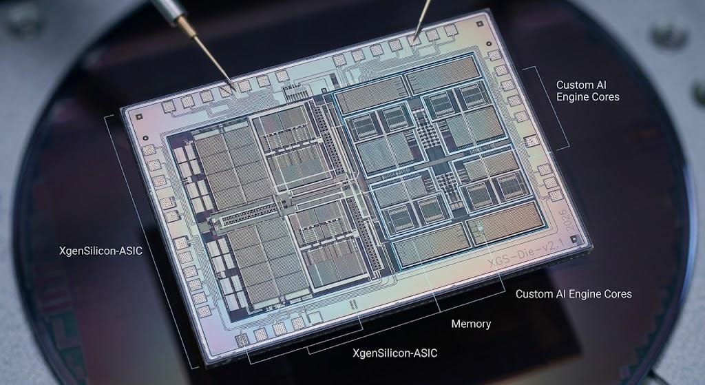
// Custom ASIC Die
Per-Model Silicon Architecture
Built to understand the exact silicon it targets. The compiler is derived from the model graph — not adapted from a generic backend — so every operator maps to the hardware it was designed for.
The AI model is the specification the hardware search runs against. Architecture candidates are evaluated against the live model graph — so the silicon is shaped by the workload from the first iteration.
A purpose-built library of silicon building blocks, each designed with its software interface in mind — so the compiler and the chip share a common language from day one.
From model ingestion to on-chip execution, the runtime is built alongside the ASIC — not ported to it. Model, software, and silicon share a single interface with no translation layers between them.
Most chip design flows treat the AI model as a fixed input — a spec handed to the compiler, which hands a spec to the hardware team. Each layer inherits constraints it had no part in setting. XgenSilicon inverts that: model architecture, software stack, and silicon are co-optimized as a single system, with every layer continuously informing every other.
Traditional
Traditional ASIC Design Flow
The model is a fixed input. Hardware specs are set without visibility into compiler needs. The compiler is written without visibility into final silicon. Each layer inherits constraints it had no part in shaping — and re-spins are the cost of discovering that late.
XgenSilicon
Model-to-Silicon Co-Design Flow
The model shapes the silicon. The silicon shapes the model. Model architecture, compiler, and hardware co-evolve — every layer has visibility into every other, so constraints are resolved at the point where they cost the least.
This diagram illustrates the structural difference in design methodology. It does not represent validated timelines or measured outcomes. XgenSilicon's Model–Software–Hardware Co-Design approach is a design-intent target; no silicon has been validated in production.
When model requirements, software architecture, and hardware specs are each locked in before the next layer can react, efficiency is lost at every boundary. XgenSilicon's platform keeps all three layers in continuous dialogue — so the compiler targets the exact silicon, and the silicon is built for the model.
We serve teams building autonomous systems, industrial robotics, personal wearables, and consumer electronics who need differentiated Edge AI products — and need them on a timeline that matters.
Reinforcement learning agents explore millions of micro-architecture candidates in simulation — evaluating power, area, and throughput tradeoffs against the live model graph — before a single gate is placed.
AI-Driven Co-Design Loop · Model-to-Silicon PPA Frontier
// AI co-design loop — runs until convergence
AI Search Agent
Explores architecture candidates
Architecture Config
Candidate hardware configuration
Fast Evaluator
Estimates PPA without full simulation
Objective Signal
Power · Performance · Area tradeoff
Agent Update
Search policy refined from feedback
// Output: Pareto-optimal PPA frontier
PPA
Optimisation objective
Power · Performance · Area
3D
Pareto frontier
All three axes simultaneously
Auto
No manual tuning required
AI-driven search
Conceptual illustration of AI-driven PPA optimisation. Axes are relative; no silicon measurements implied.
An exploration of AI-driven approaches to ASIC hardware architecture — from model specification to silicon.
Read ArticleOur latest research on AI-driven optimization techniques for neural network compilation targeting edge ASICs.
Read ArticleA comprehensive breakdown of the key performance indicators that matter most when benchmarking edge AI silicon.
Read ArticleExploring the case for custom silicon as the path to efficient, private, and low-latency LLM inference at the edge.
Read ArticleExplore the technical foundations of our System Software stack and custom ASIC platform — the Model–Software–Hardware Co-Design methodology in full detail.
Tell us about your edge AI application. We'll show you how Model–Software–Hardware Co-Design — aligning the model, System Software stack, and custom ASIC from day one — can get you to silicon faster and more efficiently.
2445 Augustine Drive, Suite 150 Santa Clara, CA, USA
